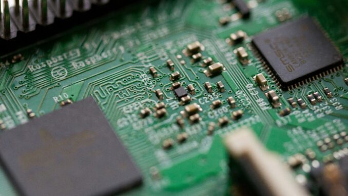
When it comes to the future of microelectronics, size does matter. And tomorrow’s microchips will need to get smaller to handle the next wave of innovations in artificial intelligence, smart devices and more, according to Seth Ariel Tongay.
Tongay is a professor in the School for Engineering of Matter, Transport and Energy (SEMTE) at Arizona State University. He has received a series of research grants from global microelectronics leader Applied Materials Inc. to create advanced technologies and help develop smaller, more energy-efficient chips.
The funding from the largest U.S. supplier of semiconductor equipment is part of a broader collaboration with ASU “to spur major breakthroughs in microelectronics,” according to the university.
For microchips, flat is where it’s at
As the semiconductor industry grapples with the shrinking returns of traditional silicon, two dimensional, or 2D, semiconductors are emerging as a bold new frontier. These materials — just a few atoms thick — promise to do what silicon no longer can: push chips to unprecedented levels of speed, efficiency and miniaturization.
Tongay and his team are venturing into the atomic-scale world to create, test and optimize materials that could soon power everything from quantum computing to rapidly advancing AI-enabled hardware.
“(Two-dimensional) semiconductors offer something traditional silicon just can’t anymore,” Tongay says. “They let us go beyond the limits of current technology, achieving ultrascaling while keeping performance high and energy use low. This is the next era of electronics. And it’s happening now.”
Unlike silicon wafers, which are relatively thick and constrained by physical boundaries, 2D semiconductors are ultra-thin, flexible and boast remarkable electronic properties. They could enable chips with layers stacked like sheets of paper, allowing engineers to fit more processing power into less space.
But making these materials at scale, with the consistency and quality demanded by industry, is no easy feat. That’s why Tongay’s team is developing new ways to grow these materials, using methods that place super-thin layers exactly where they’re needed on a chip, almost like printing with atoms.
“We’re not just making materials,” Tongay says. “We’re architecting them with precision, atom by atom, location by location.”
Once grown, the materials will undergo rigorous performance testing, where they will be benchmarked against tried-and-true semiconductors made from silicon and silicon-germanium. The goal is to demonstrate that 2D materials can not only compete with, but in some cases surpass, their older counterparts.
The team’s work isn’t about replacing silicon — it’s about leapfrogging it. Two-dimensional semiconductors aren’t only thinner, they behave differently. They can be tuned for new types of transistors, enable flexible electronics and even open doors to photonic or spintronic computing.
Anthony Tam, a business development director for ASU’s Fulton Schools of Engineering, says the implications extend far beyond academia.
“What’s so exciting about this work is that it directly tackles a critical industry challenge: How do we keep scaling advanced chips while driving down power consumption?” Tam says. “Future AI processors could draw more than 10 kilowatts, equivalent to the energy usage of 1,000 household light bulbs. This project has the potential to be a game-changing breakthrough.”
The projects could help usher in a new wave of electronics — smaller, faster, cooler-running devices that are also more energy efficient. Think wearables that last days on a single charge, AI processors with lightning-fast performance or data centers that don’t require a city’s worth of power to operate.
The thin edge of tomorrow
To create these atom-thin materials, Tongay’s team is developing new techniques to grow them directly onto chip surfaces — one atomic layer at a time. This bottom-up method offers far greater precision than traditional approaches, enabling fine-tuned control over the structure and performance of each layer.
The team is using advanced methods such as pulsed laser deposition, or PLD, and plasma-enhanced chemical vapor deposition, or PECVD, to make it happen. In PLD, a powerful laser blasts a solid material into a plasma, which then settles into a thin film on a heated surface. PECVD, on the other hand, uses energized gases to trigger chemical reactions that build up layers at lower temperatures.
“We’re working to make sure these cutting-edge materials can actually be used in the real world,” Tongay says. “That means improving performance, but also making them easier to grow, test and scale.”
